- 您现在的位置:买卖IC网 > Sheet目录3818 > PIC18F4620-I/ML (Microchip Technology)IC MCU FLASH 32KX16 44QFN
PIC17C4X
DS30412C-page 42
1996 Microchip Technology Inc.
6.8
Bank Select Register (BSR)
The BSR is used to switch between banks in the data
memory
area
In
the
PIC17C42,
PIC17CR42, and PIC17C42A only the lower nibble is
implemented. While in the PIC17C43, PIC17CR43,
and PIC17C44 devices, the entire byte is implemented.
The lower nibble is used to select the peripheral regis-
ter bank. The upper nibble is used to select the general
purpose memory bank.
All the Special Function Registers (SFRs) are mapped
into the data memory space. In order to accommodate
the large number of registers, a banking scheme has
been used. A segment of the SFRs, from address 10h
to address 17h, is banked. The lower nibble of the bank
select register (BSR) selects the currently active
“peripheral bank.” Effort has been made to group the
peripheral registers of related functionality in one bank.
However, it will still be necessary to switch from bank
to bank in order to address all peripherals related to a
single task. To assist this, a MOVLB bank instruction is
in the instruction set.
For the PIC17C43, PIC17CR43, and PIC17C44
devices, the need for a large general purpose memory
space dictated a general purpose RAM banking
scheme. The upper nibble of the BSR selects the cur-
rently active general purpose RAM bank. To assist this,
a MOVLR bank instruction has been provided in the
instruction set.
If the currently selected bank is not implemented (such
as Bank 13), any read will read all '0's. Any write is com-
pleted to the bit bucket and the ALU status bits will be
set/cleared as appropriate.
Note:
Registers in Bank 15 in the Special Func-
tion
Register
area,
are
reserved
for
Microchip use. Reading of registers in this
bank may cause random values to be read.
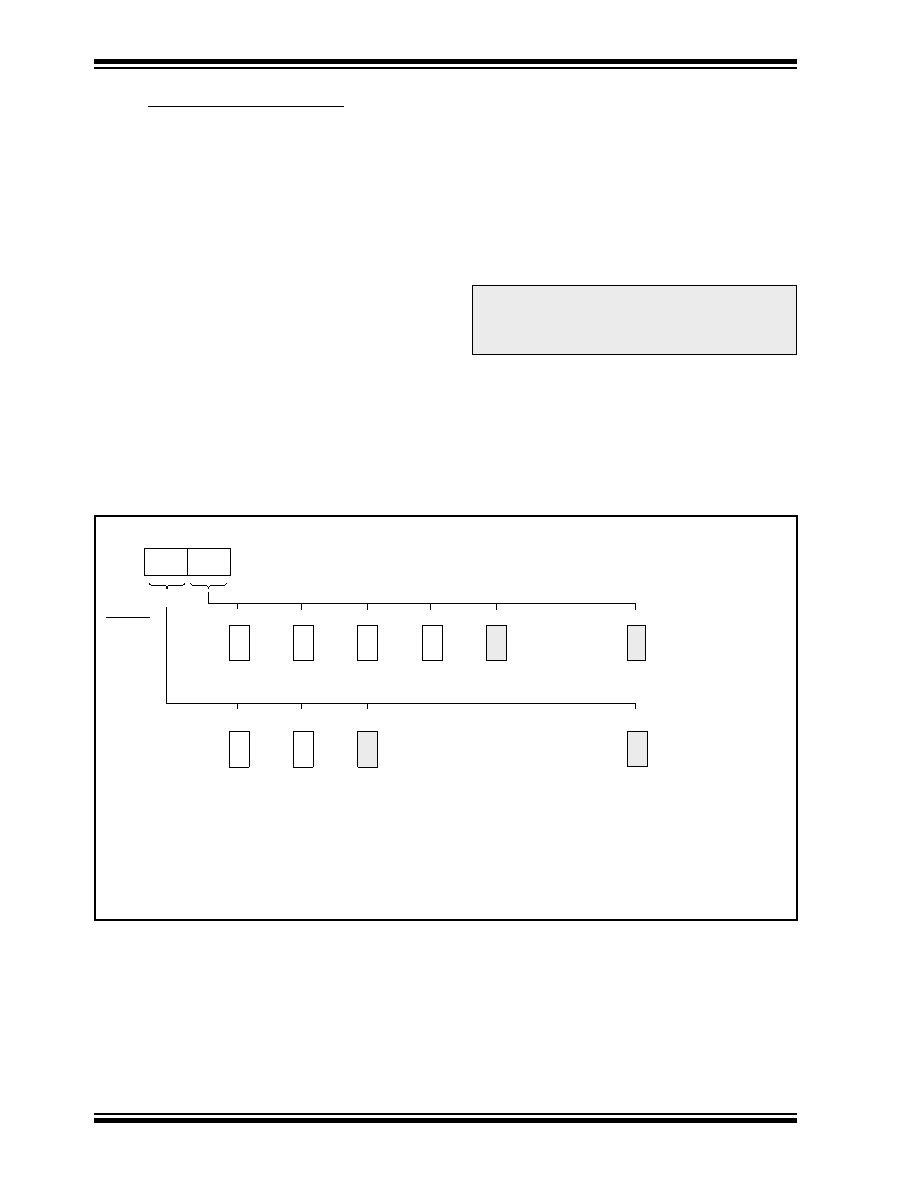
FIGURE 6-13: BSR OPERATION (PIC17C43/R43/44)
74 3
0
10h
17h
BSR
01
2
3
4
15
20h
FFh
(1)
(2)
Bank 15
Bank 4
Bank 3
Bank 2
Bank 1
Bank 0
01
2
Bank 2
Bank 1
Bank 0
15
Bank 15
SFR
Banks
GPR
Banks
Address
Range
Note 1:
Only Banks 0 through Bank 3 are implemented. Selection of an unimplemented bank is not recommended.
Bank 15 is reserved for Microchip use, reading of registers in this bank may cause random values to be read.
2:
Only Banks 0 and Bank 1 are implemented. Selection of an unimplemented bank is not recommended.
发布紧急采购,3分钟左右您将得到回复。
相关PDF资料
PIC24HJ256GP210-I/PT
IC PIC MCU FLASH 128KX16 100TQFP
PIC24HJ128GP310A-I/PF
IC PIC MCU FLASH 128KB 100-TQFP
DSPIC33FJ128GP310-I/PF
IC DSPIC MCU/DSP 128K 100TQFP
PIC16C66-20I/SO
IC MCU OTP 8KX14 PWM 28SOIC
DSPIC33FJ128MC510-I/PT
IC DSPIC MCU/DSP 128K 100TQFP
PIC16C66-20I/SP
IC MCU OTP 8KX14 PWM 28DIP
PIC18LF2620-I/SP
IC MCU FLASH 32KX16 28SDIP
PIC16F877-04I/P
IC MCU FLASH 8KX14 EE 40DIP
相关代理商/技术参数
PIC18F4620-I/P
功能描述:8位微控制器 -MCU 64KB 3968 RAM 36 I/O RoHS:否 制造商:Silicon Labs 核心:8051 处理器系列:C8051F39x 数据总线宽度:8 bit 最大时钟频率:50 MHz 程序存储器大小:16 KB 数据 RAM 大小:1 KB 片上 ADC:Yes 工作电源电压:1.8 V to 3.6 V 工作温度范围:- 40 C to + 105 C 封装 / 箱体:QFN-20 安装风格:SMD/SMT
PIC18F4620-I/P
制造商:Microchip Technology Inc 功能描述:IC 8BIT FLASH MCU 18F4620 DIP40
PIC18F4620-I/PT
功能描述:8位微控制器 -MCU 64KB 3968 RAM 36 I/O RoHS:否 制造商:Silicon Labs 核心:8051 处理器系列:C8051F39x 数据总线宽度:8 bit 最大时钟频率:50 MHz 程序存储器大小:16 KB 数据 RAM 大小:1 KB 片上 ADC:Yes 工作电源电压:1.8 V to 3.6 V 工作温度范围:- 40 C to + 105 C 封装 / 箱体:QFN-20 安装风格:SMD/SMT
PIC18F4620-I/PT
制造商:Microchip Technology Inc 功能描述:IC 8BIT FLASH MCU 18F4620 TQFP44
PIC18F4620T-I/ML
功能描述:8位微控制器 -MCU 64KB 3968 RAM 36 I/O RoHS:否 制造商:Silicon Labs 核心:8051 处理器系列:C8051F39x 数据总线宽度:8 bit 最大时钟频率:50 MHz 程序存储器大小:16 KB 数据 RAM 大小:1 KB 片上 ADC:Yes 工作电源电压:1.8 V to 3.6 V 工作温度范围:- 40 C to + 105 C 封装 / 箱体:QFN-20 安装风格:SMD/SMT
PIC18F4620T-I/PT
功能描述:8位微控制器 -MCU 64KB 3968 RAM 36 I/O RoHS:否 制造商:Silicon Labs 核心:8051 处理器系列:C8051F39x 数据总线宽度:8 bit 最大时钟频率:50 MHz 程序存储器大小:16 KB 数据 RAM 大小:1 KB 片上 ADC:Yes 工作电源电压:1.8 V to 3.6 V 工作温度范围:- 40 C to + 105 C 封装 / 箱体:QFN-20 安装风格:SMD/SMT
PIC18F4680-E/ML
功能描述:8位微控制器 -MCU 64KB 3328 RAM w/ECAN RoHS:否 制造商:Silicon Labs 核心:8051 处理器系列:C8051F39x 数据总线宽度:8 bit 最大时钟频率:50 MHz 程序存储器大小:16 KB 数据 RAM 大小:1 KB 片上 ADC:Yes 工作电源电压:1.8 V to 3.6 V 工作温度范围:- 40 C to + 105 C 封装 / 箱体:QFN-20 安装风格:SMD/SMT
PIC18F4680-E/P
功能描述:8位微控制器 -MCU 64KB 3328 RAM w/ECAN RoHS:否 制造商:Silicon Labs 核心:8051 处理器系列:C8051F39x 数据总线宽度:8 bit 最大时钟频率:50 MHz 程序存储器大小:16 KB 数据 RAM 大小:1 KB 片上 ADC:Yes 工作电源电压:1.8 V to 3.6 V 工作温度范围:- 40 C to + 105 C 封装 / 箱体:QFN-20 安装风格:SMD/SMT